The quest for unblemished optical clarity—the ability to see through a transparent medium without the distraction of glare or the diminishment of light—has driven significant advancements in materials science and thin-film technology. Central to this pursuit is the application of the anti-reflective (AR) coating to optical components, particularly high-performance crystals used in everything from precision scientific instruments to high-end consumer electronics. The process is far more intricate than a simple surface layer; it is a meticulously controlled ballet of physics, chemistry, and engineering, executed in an ultra-clean, high-vacuum environment. The resulting coating doesn’t just reduce reflection; it actively manipulates the behavior of light waves, achieving near-perfect transmission across a defined spectrum.
The Principle of Interference: How AR Coatings Work
To truly appreciate the complexity of the application process, one must first grasp the core principle underpinning AR coating function: wave interference. When light strikes the surface of an uncoated crystal, a portion is reflected due to the sudden change in the refractive index between the air and the crystal material. For typical glass, this reflection loss is about 4% per surface, which quickly compounds in multi-element optical systems.
An AR coating, typically a stack of alternating thin-film layers with varying refractive indices, mitigates this reflection. The thickness and refractive index of each layer are calculated with extreme precision to ensure that light waves reflected from the various interfaces (air-coating, coating-coating, coating-crystal) are out of phase with one another. When these out-of-phase waves recombine, they undergo destructive interference, effectively cancelling each other out. This cancellation eliminates the reflected light, meaning more light is transmitted through the crystal, thus boosting throughput and eliminating ghosting or flare.
The fundamental mechanism of an anti-reflective coating relies on destructive interference. By depositing thin films with specific optical thicknesses (an odd multiple of a quarter of the target wavelength), light waves reflected from the top and bottom of the layer are made to travel a half-wavelength path difference, ensuring they cancel each other out upon re-emission, resulting in minimal reflection and maximum transmission.
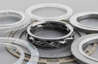
The design varies considerably based on the application. A simple single-layer coating like magnesium fluoride (MgF2) is optimized for a narrow wavelength band, often exhibiting a characteristic “V-shape” reflectivity curve. Conversely, modern broadband anti-reflective (BBAR) coatings employ complex stacks of up to seven or more layers, engineered to maintain low reflectivity across the entire visible spectrum or beyond (UV/IR), necessitating even tighter control over layer thickness.
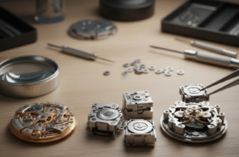
Stage One: Preparation of the Crystal Substrate
The success of an AR coating hinges almost entirely on the cleanliness and preparedness of the crystal substrate. The adhesion and optical performance of the ultra-thin films are extraordinarily sensitive to even microscopic contaminants.
Initial Cleaning and Inspection
The crystal, often a delicate material like synthetic sapphire, fused silica, or specialized optical glass, undergoes a rigorous multi-stage cleaning protocol. This typically includes:
- Ultrasonic Cleaning: Immersion in a series of baths with specialized detergents, where high-frequency sound waves agitate the liquid, dislodging particulate matter and organic residues.
- Rinsing: Repeated rinsing in high-purity, deionized (DI) water to remove all traces of cleaning agents and minerals.
- Vapor Degreasing/Solvent Cleaning: Utilizing specialized, volatile solvents in a vapor phase to dissolve any remaining oils or greases from the polishing process.
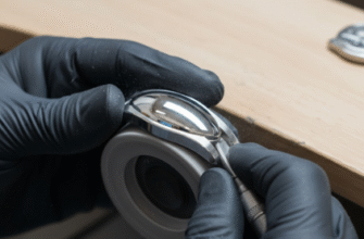
After cleaning, the crystals are meticulously inspected under high magnification. Any remaining flaw, smudge, or particle can create a point defect in the final coating, leading to scattering losses or, worse, a site for laser-induced damage in high-power applications. Proper handling is critical, usually involving specialized tweezers and personnel operating in a Class 100 or better cleanroom environment.
Fixture and Mounting
The prepared crystals must be securely mounted onto specialized fixtures or calottes within the coating chamber. This fixturing must ensure:
- Consistent positioning relative to the vapor source.
- Maximum surface area exposure for coating uniformity.
- Robustness to withstand the high temperatures and ion bombardment of the vacuum process.
Stage Two: High-Vacuum Deposition Technology
The actual application of the coating layers is carried out using vacuum deposition techniques, most commonly Physical Vapor Deposition (PVD) methods like electron beam evaporation or magnetron sputtering. These processes occur within a large, sealed vacuum chamber to prevent atmospheric gases from contaminating the deposited films.
Achieving Deep Vacuum
The first critical step in the chamber is achieving an extremely low base pressure, often below 10−6 Torr. High-speed vacuum pumps—a combination of roughing pumps, turbo-molecular pumps, and often cryopumps—are used to pull a deep vacuum. This hyper-low pressure is necessary to ensure that the atoms or molecules of the coating material can travel unimpeded from the source to the crystal surface without colliding with residual gas molecules—a condition called a long mean free path.
The Deposition Method: Electron-Beam Evaporation
A widely used PVD technique is Electron-Beam Evaporation (E-beam Evaporation). The process involves:
- The coating material (e.g., SiO2, TiO2, Ta2O5) is placed in crucibles within the chamber.
- A high-energy electron beam is focused onto the material, causing it to heat rapidly and vaporize.
- The vaporized material travels as a plume of individual atoms or molecules.
- These particles condense and adhere to the cooler crystal substrates, forming a solid, thin film.
In high-precision applications, this is often assisted by Ion-Assisted Deposition (IAD), where an ion gun bombards the growing film with inert gas ions (like Argon) to pack the coating material more densely. This increases the film’s hardness, chemical resistance, and environmental stability, preventing the film’s refractive index from shifting due to atmospheric moisture absorption.
Magnetron Sputtering
Another dominant method is Magnetron Sputtering, particularly favored for its ability to produce highly dense and uniform films with excellent adhesion. In this process:
- The coating material (the “target”) is struck by high-energy plasma ions.
- This collision physically ejects or “sputters” atoms from the target material.
- These sputtered atoms then deposit onto the crystal.
Sputtering offers superior control and consistency for multi-layer stacks, a necessity for complex BBAR designs.
Precision in deposition is paramount: a deviation in layer thickness of even a few nanometers can drastically shift the coating’s optimized wavelength, rendering it ineffective. Continuous monitoring via quartz crystal monitors and optical thickness monitors is vital to ensure the physical thickness of each layer corresponds precisely to the required optical quarter-wave thickness (λ/4).
Stage Three: Real-Time Monitoring and Layer Stacking
Optical Thickness Monitoring (OTM)
During deposition, the growth of the film is monitored in real-time. The most advanced method is OTM, which uses a reference light source directed at a witness sample inside the chamber. As the film grows, light reflecting from the surface changes in intensity due to interference. The system detects the points of maximum and minimum reflection (the “turning points”), which correspond to precise optical thicknesses (λ/4 or λ/2 multiples). The deposition is halted precisely at the target turning point for each layer before the next material is introduced.
The Layer Sequence
A typical multi-layer AR coating involves the alternating deposition of two materials: one with a relatively high refractive index (H) and one with a low refractive index (L). Common materials include TiO2 or Ta2O5 for the high index layers and SiO2 for the low index layers. The stack might look like Air/L/H/L/H/L/Crystal, with the outermost layer typically having a refractive index closest to that of air to provide the final phase cancellation for maximum transmission.
Stage Four: Post-Deposition Hardening and Finishing
Curing and Post-Treatment
Once all layers have been deposited, the crystal is removed from the vacuum chamber. Depending on the process, some coatings, especially those with organic components or those made via Plasma-Enhanced Chemical Vapor Deposition (PECVD) or sol-gel methods, may require a final curing stage, such as baking in a clean oven or exposure to Ultraviolet (UV) light, to fully harden the film and enhance its structural integrity. For high-durability military or industrial optics, additional plasma or ion beam post-treatment might be applied to further densify the surface.
Quality Control and Testing
The finished crystal undergoes a final, rigorous suite of quality control tests:
- Spectrophotometry: Measures the crystal’s actual transmission and reflection curves across the required wavelength band to confirm the optical performance meets the design specification (e.g., reflection below 0.25% average).
- Adhesion Testing: Uses a cross-hatch or tape-pull test to verify the coating’s mechanical bond to the substrate.
- Durability Testing: Includes abrasion (cheesecloth or specified eraser rub) and environmental tests (exposure to humidity and temperature extremes) to ensure the coating’s longevity and resistance to handling and operation conditions.
Only crystals that pass all these checks are deemed finished, ready for integration into their final system, delivering the clear, high-contrast vision that the complex AR coating process was designed to provide.